MBE Arsenic
Quantum Hall effects (high-mobility samples), cleaved-edge overgrowth (CEO), and advanced gating (ion implantation)
Next to silicon, GaAs/AlAs is one of the most significant and well-understood material systems in semiconductor physics. Being common in many different application fields, e.g., in communications such as cell phones or satellites, high-efficiency photovoltaics, and laser technology, As-based semiconductor heterostructures are currently investigated by many research groups. From a more fundamental point of view, high-quality III/V compound semiconductor heterostructures are a basis to study the physics of correlated electrons in systems of reduced dimension.
We fabricate complex GaAs/AlGaAs heterojunctions using MBE with single-atom-layer precision. Perpetual optimization of the MBE growth to improve the charge-carrier mobility and overall sample performances is one key research area within our group.
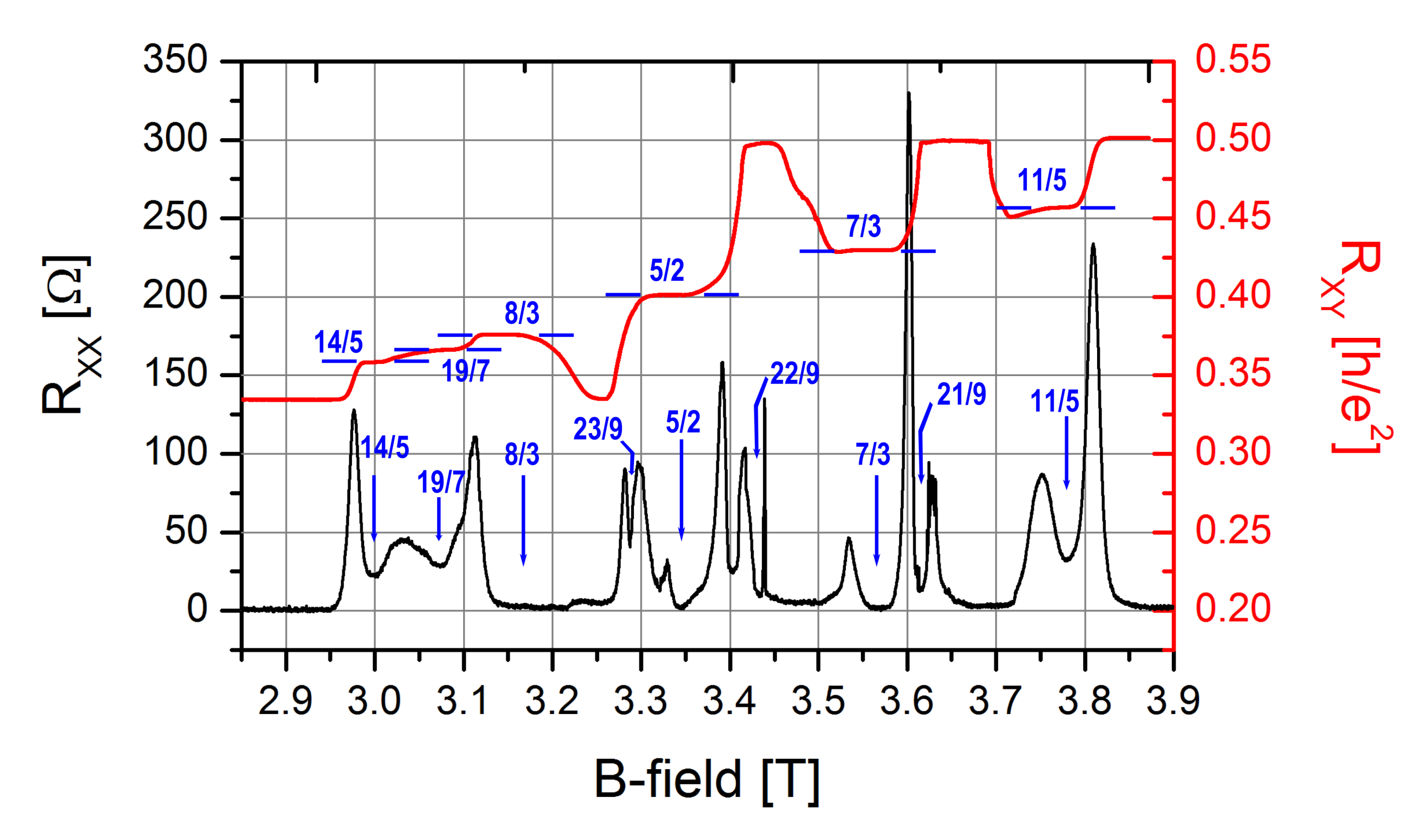
Samples with very high mobility are the foundation to observe a multitude of fragile fractional quantum Hall states (FQHS). The number of defects and impurities incorporated during the MBE growth process needs to be minimized, while the material composition needs to be optimized to obtain the highest-mobility samples. As the potential disorder created by remote ionized donors is currently considered to be the main factor prohibiting the development of FQH states, and especially the ν = 5/2 state, we continue our efforts to reduce the impact of remote ionized impurities on the magnetotransport properties.
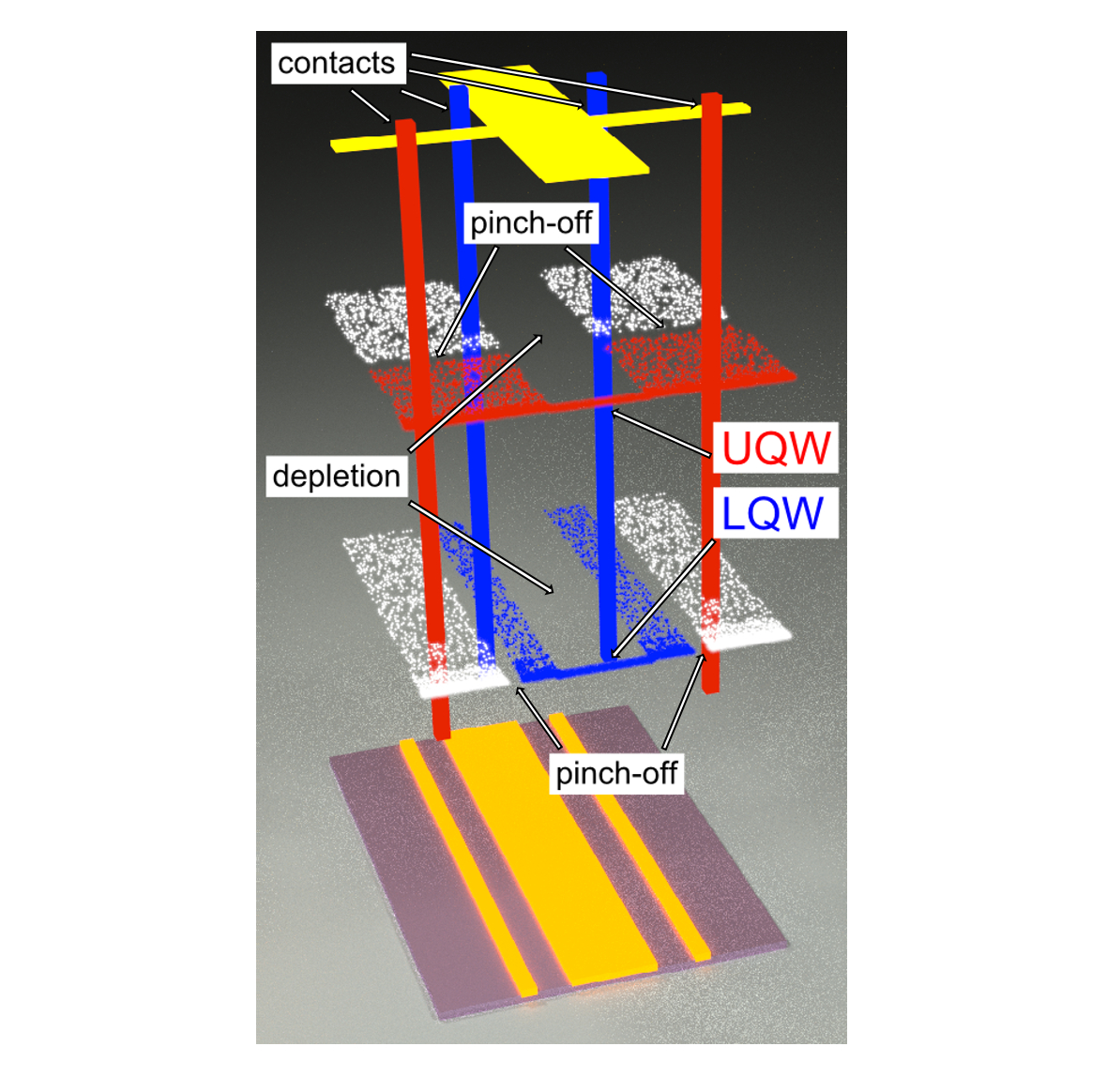
For flexible control and spatial definition of 2DEGs, gating techniques are a powerful tool. We focus on gating technologies that are suitable to combine with MBE. This technology allows us to produce structured (buried) back gates that are overgrown by a desired heterostructure. Additionally, since modulated doping has a large impact on the quality of the highest-mobility 2DEGs, we also produce and investigate gate-induced electron systems.
The study of the one-dimensional (1D) physics of cleaved-edge overgrowth (CEO) [Deutschmann01,Wegscheider06] quantum wires (QWRs) using AlGaAs/GaAs molecular-beam epitaxy (MBE) is another current project. These very pure and atomically precise quantum systems are expected to reveal new physics of 1D Luttinger liquids. In particular, we are interested in the creation of separately gateable coupled QWRs.
[Deutschmann01]: R. A. Deutschmann, W. Wegscheider, M. Rother, M. Bichler, G. Abstreiter, Phys. Rev. Lett. 86, 1857-1860 (2001).
[Wegscheider06]: W. Wegscheider, M. Rother, R. Deutschmann, T. Feil, physica status solidi (b) 243 (2006).
Indium arsenide quantum dots
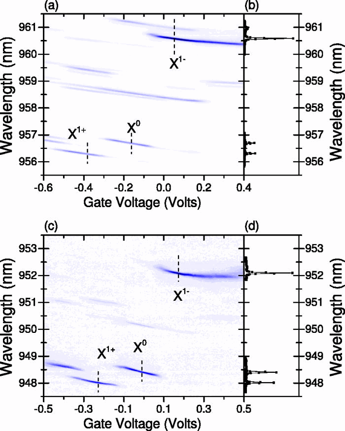
A self-assembled InAs quantum dot (QD) in GaAs allows confinement of carriers in all directions and the formation of a 0-dimensional "artificial atom". With the addition of gates [Kinnischtzke16], the QD can be charged with electrons or holes, which can be identified by shifts in the optical transition in the QD (see figure).
The spin of a single electron [Vamivakas10] or hole [Delteil15] in the QD can be used as a qubit. We aim to improve the material quality and structure of the epitaxially grown QDs. One approach is to use tunnel-coupled QDs charged with two electrons and use the singlet and triplet spin configurations, as these are protected from magnetic and electric decoherence processes [Delley15].
[Kinnischtzke16] L. Kinnischtzke et al., Appl. Phys. Lett. 108, 211905 (2016).
[Vamivakas10] A. N. Vamivakas et al., Nature 467, 297 (2010).
[Delteil15] A. Delteil et al., Nature Physics 12, 218 (2015).
[Delley15] Y. L. Delley et al., arXiv:1509.04171 [cond-mat.mes-hall]